Linx
How to Use the LC Series LINX Modules
by Lee RumseyThese are basic instructions on hooking up the modules. This document is split into five nifty sections:
For data sheets on the LINX modules, see this web site: http://www.linxtechnologies.com. Click on the RF Modules link. Then click on the Manuals item under the LC Series heading. READ through the LC Series data sheets to get an understanding of their function. This will reduce the likelihood of errors.
Necessary Parts
Before we start
- Learn to solder. You will be making some delicate connections, so practice if you don't know how. Also be sure to use solder sparingly- big blobs will likely result in damage or malfunctions.
- You should have the parts listed above. Get them from a TA.
- Make sure the transmitter and receiver are running on the same frequency. Do this by checking the model number on the surface mount package. For example, a 418 MHz TX module will be labeled TXM-418-LC, and a 315 MHz RX module will be RXM-315-LC.
Transmitter Assembly
The LINX transmitter is the smaller of the two modules. It runs on between +2.7 and 5.2 VDC. We will use a +5 VDC power supply, so that the data input can be a TTL level signal. DO NOT apply a voltage greater than Vcc on the data input pin!
Step 1. Acclimate yourself with the circuit we are building:
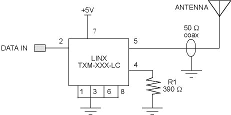
Step 2. Place the TX board with chip side facing UP. The writing on the chip should be right side up, with a little wire coming off the top. This wire is GROUND. A '1' or a small dot should be visible on the lower left-hand corner of the chip. GROUND is also connected to the center bus strip on the board.
Step 3. Solder the 390 W resistor from pin 4 (lower right-hand corner) to ground. This sets the chip to accept 5 VDC. NOTE: make all connections on the top of the board. DON'T feed any leads through the holes. There are connections on the other side!
Step 4. Carefully solder a 3-inch wire to pin 2. This will be the DATA input. DO NOT apply a voltage greater than Vcc on the data input pin!
Step 5. Carefully solder a 3-inch wire to pin 7. This will be the VCC power input. REMEMBER: +5 VDC ONLY on this pin!
Step 6a. If you have a HELICAL COIL antenna, solder a short (2 inch) length of coax cable to pin 5 and GROUND. The inner conductor is the RF signal, and the outer shield goes to GROUND. Now solder the helical coil to the other end of the coax to form a magnetic loop. (You may need to extend the shield connection with a separate wire.)
Step 6b. If you have a WHIP antenna, solder the coax cable directly to pin 5 and GROUND. The inner conductor is the RF signal, and the outer shield goes to GROUND.
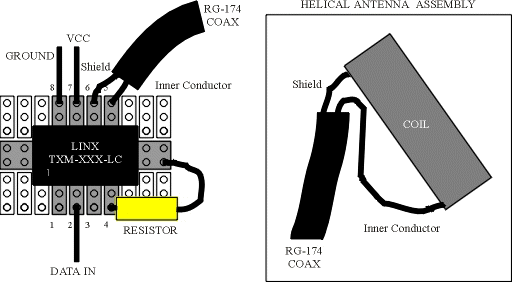
Here is the completed TX board assembly:
Receiver Assembly
The LINX receiver is the larger of the two modules. It runs on between +4 and 5.2 VDC. We will use a +5 VDC power supply. GROUND is the center vertical strip on the solder side.
Step 1. Acclimate yourself with the circuit we are building:
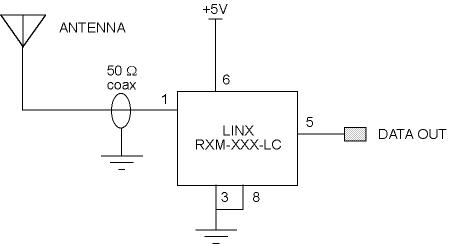
Step 2. Place the RX board with chip side facing DOWN, with the solder side UP. Orient the board so that one wire comes off the top, while another comes off the left of the board. The top wire is the power connection; the left wire is ground. Pin 1 of the chip is actually at the lower left with this orientation; it is identified on the chip by a '1' or a dot.
Step 3. Carefully solder a 3-inch wire to pin 5 (top left solder pad connected to the chip). This will be the DATA output.
Step 4a. If you have a HELICAL COIL antenna, solder a short (2 inch) length of coax cable to pin 1 and GROUND. The inner conductor is the RF signal, and the outer shield goes to GROUND. Now solder the helical coil to the other end of the coax to form a magnetic loop. (You may need to extend the shield connection with a separate wire.)
Step 4b. If you have a WHIP antenna, solder the coax cable directly to pin 1 and GROUND. The inner conductor is the RF signal, and the outer shield goes to GROUND.
Step 5. IMPORTANT! If there is a connection to pin 10 on the Linx chip, carefully desolder it, leaving the others intact. It is misconnected.
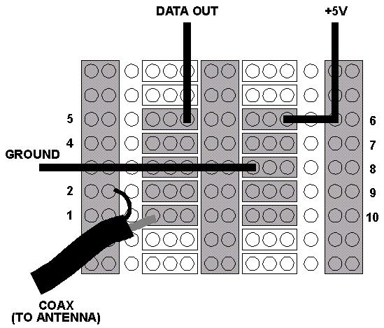
Here is the completed RX board assembly:
Testing and Operation
Now we'll see if these modules work. If you are working with 418 MHz chips, then a reference receiver - transmitter pair are available for testing. Otherwise, you better hope you made the right connections? we don't have anything to test the 315 MHz RX/TX chips, except maybe another functioning pair of modules.Step 1. TESTING THE TRANSMITTER. Refer to the schematic for the TX module we just assembled. Connect +5 VDC to the power lead, and ground the GROUND lead.
Step 2. Turn on or plug in the power. Use +5 VDC only! If anything is heating up, UNPLUG the module and check your connections!
Step 3. Set up a function generator the make a 1 kHz TTL compatible square wave (i.e. it swings between 0 and +5V only!) Connect this signal to the data input lead from the module. If anything is heating up, UNPLUG the module and check your connections!
Step 4. Plug the data output of the reference receiver into an oscilloscope. ASK A TA FOR ASSISTANCE! If all is well, a 1 kHz square wave should appear on the screen. You are done; wire your module into the rest of your circuit.
NOTE: For a flaky power supply, a bypass capacitor (10 uF electrolytic) may be necessary between power and ground on YOUR board.
Step 5. TESTING THE RECEIVER. Refer to the schematic for the RX module we just assembled. Connect +5 VDC to the power lead, and ground the GROUND lead
Step 6. Turn on or plug in the power. Use +5 VDC only! If anything is heating up, UNPLUG the module and check your connections!
Step 7. Set up a function generator the make a 1 kHz TTL compatible square wave (i.e. it swings between 0 and +5V only!) Connect this signal to the data input on the reference transmitter. ASK A TA FOR ASSISTANCE! If anything is heating up, UNPLUG the module and check your connections!
Step 8. Connect the data output of your receiver module into an oscilloscope. If all is well, a 1 kHz square wave should appear on the screen. You are done; wire your module into the rest of your circuit.
THE END.