ECE 486 Control Systems
Lecture 17
Control Design Using Frequency Response (Continued)
Last time, we used Bode’s Gain-Phase Relationship as a guideline for control design using frequency response. One of our attempts during the time was designing a lead controller for a double integrator.
In this lecture, we will continue our discussion of control design using frequency response; we shall explore other design options such as PI/lag, PID/lead+lag.
Lag Compensation in Bode Plot
Similar to lead controller we considered last time, here we consider a lag compensator as in Equation \eqref{d17_eq1}.
\begin{align*} \tag{1} \label{d17_eq1} D(s) &= \dfrac{s+z}{s+p} \\ &= \frac{z}{p} \frac{\frac{s}{z}+1}{\frac{s}{p}+1}, \end{align*}where \(z \gg p\), hence the lag control.
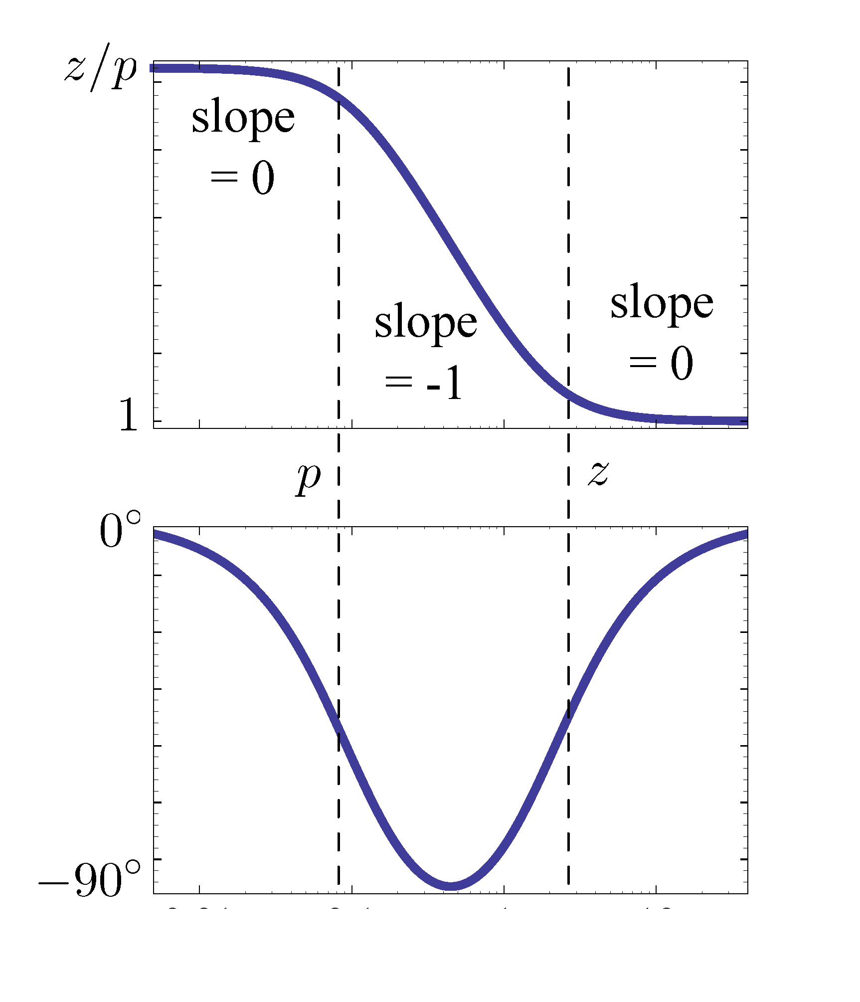
Figure 1: Bode plot for lag component \(D(s) = \frac{s+z}{s+p}\)
From Figure 1, we notice
- \(z \gg p\) means \(\angle s+z < \angle s+p\), hence the term “phase lag”.
- \(\dfrac{j\omega+z}{j\omega+p} \to 1\) as \(\omega \to \infty\), so magnitude \(M \to 1\) at high frequencies.
- \(\dfrac{j\omega+z}{j\omega+p} \to \frac{z}{p}\) as \(\omega \to 0\). By the calculation of steady state tracking error \[ \left. e(\infty) = \frac{sR(s)}{1+D(s)G(s)} \right|_{s=0}, \] we see large \(\frac{z}p\) means better tracking. It is essentially confirming lag control as approximate PI control can be used to suppress steady state error.
- By the magnitude plot, the lag component steps down slope by \(-1\) so lag control decreases \(\omega_c\); it further implies it slows down time response. (Why? Hint: Recall the relationship among bandwidth \(\omega_{\rm BW}\), crossover frequency \(\omega_c\) and natural frequency \(\omega_n\).)
- Contrary to lead control which increases PM, lag control can undo what lead control does. To mitigate this, choose both \(z\) and \(p\) to be very small, while maintaining desired ratio \(\frac{z}p\) so that we can keep the benefit of lag control.
Consider the following example. Let \(G(s) = \frac{1}{(s+0.2)(s+0.5)}\). Write it in Bode form,
\begin{align*} G(s) &= \frac{1}{(s+0.2)(s+0.5)} \\ &= \frac{10}{s^0}\cdot\frac{1}{\left(\frac{s}{0.2}+1\right)\left(\frac{s}{0.5}+1\right)}. \end{align*}Our objectives include
- phase margin \({\rm PM} \ge 60^\circ\);
- steady state error \(e(\infty) \le 10\%\) for tracking constant reference input. (This is closed loop tracking error.)
Our strategy here is to use a lag controller to achieve the above requirements
\[ KD(s) = K\frac{s+z}{s+p}, \text{ where } z \gg p. \]
On top of the lag control in this form, we further require that
- \(z\) and \(p\) be chosen to get good tracking;
- phase margin be shaped by choosing \(K\).
As for shaping phase margin, note that this is different from what we did for using lead control where we chose \(K\) to get desired bandwidth specification and used \(p\) and \(z\) to shape phase margin \(\rm{PM}\).
Step 1: Choose \(K\) to Shape Phase Margin \(\rm{PM}\)
First check the Bode plot of \(G(s)\) to see the existing phase margin from it.
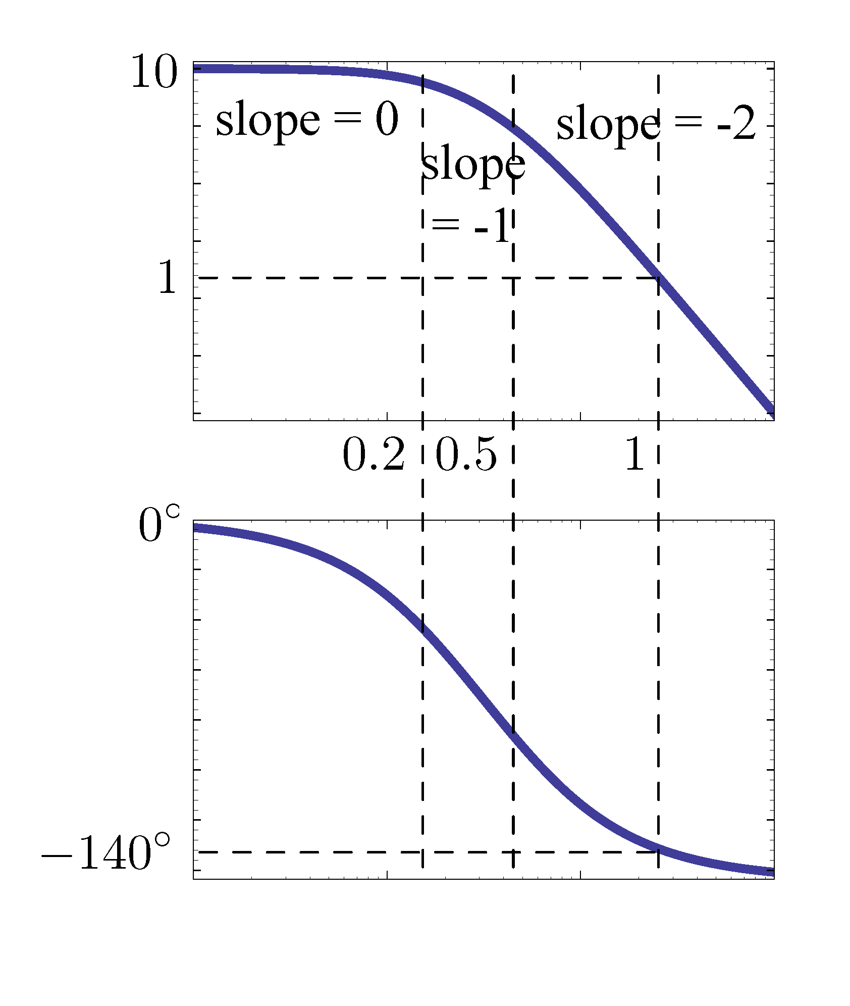
Figure 2: Bode plot for \(G(s)\) only
From Matlab, we see
- crossover frequency \(\omega_c \approx 1\);
- phase margin \(\text{PM} \approx 40^\circ\) but the desired phase margin is at least \(\text{PM} = 60^\circ\);
- from phase plot of Figure 2, \(\angle G(j\omega) = -120^\circ\) at \(\omega \approx 0.573\). The corresponding magnitude is \(|G(j\omega)| = 2.16\). So we can choose \(K\) to be \(\frac{1}{2.16}\). (Move magnitude graph down to push crossover frequency down.)
A conservative choice (to allow some slack) could be \(K = \frac{1}{2.5} =0.4\), which gives \(\omega_c \approx 0.52,\, \text{PM} \approx 65^\circ\).
Step 2: Choose \(z\) and \(p\) to Shape Tracking Error
After we determined \(K = 0.4\) in Step 1, we have
\[ KG(s) = \dfrac{0.4 \cdot 10}{\left(\frac{s}{0.2}+1\right)\left(\frac{s}{0.5}+1\right)}. \]
If we do nothing to the above transfer function \(KG(s)\), the steady state error would be
\begin{align*} e(\infty) &= \left. \frac{1}{1 + KG(s)}\right|_{s=0} \\ &= \frac{1}{1+4} \\ &= \frac{1}{5} \\ &= 20\% > 10\%. \end{align*}To have \(e(\infty) \le 10\%\) as specified, we need \(KD(0)G(0) \ge 9\) since
\begin{align*} e(\infty) &= \frac{1}{1+KD(0)G(0)} \le \frac{1}{1+9} \\ &= 10\%. \end{align*}Therefore,
\begin{align*} D(0) &= \left. \frac{s+z}{s+p}\right|_{s=0} \\ &= \frac{z}{p} \ge \frac{9}{4} \\ &= 2.25. \end{align*}We can choose \(\frac{z}p = 2.5\). Recall in order not to distort phase margin and \(\omega_c\), we can pick \(z\) and \(p\) an order of magnitude smaller than \(\omega_c \approx 0.5\), e.g., \(z = 0.05\), \(p = 0.02\).
Overall Design
After we completed Step 1 and 2, the controller is determined as
\[ KD(s) = 0.4 \frac{s+0.05}{s+0.02} \]
for plant
\[ G(s) = \dfrac{10}{\left(\dfrac{s}{0.2}+1\right)\left(\dfrac{s}{0.5}+1\right)}. \]
The Bode plot for \(KD(s)G(s)\) is shown in Figure 3.
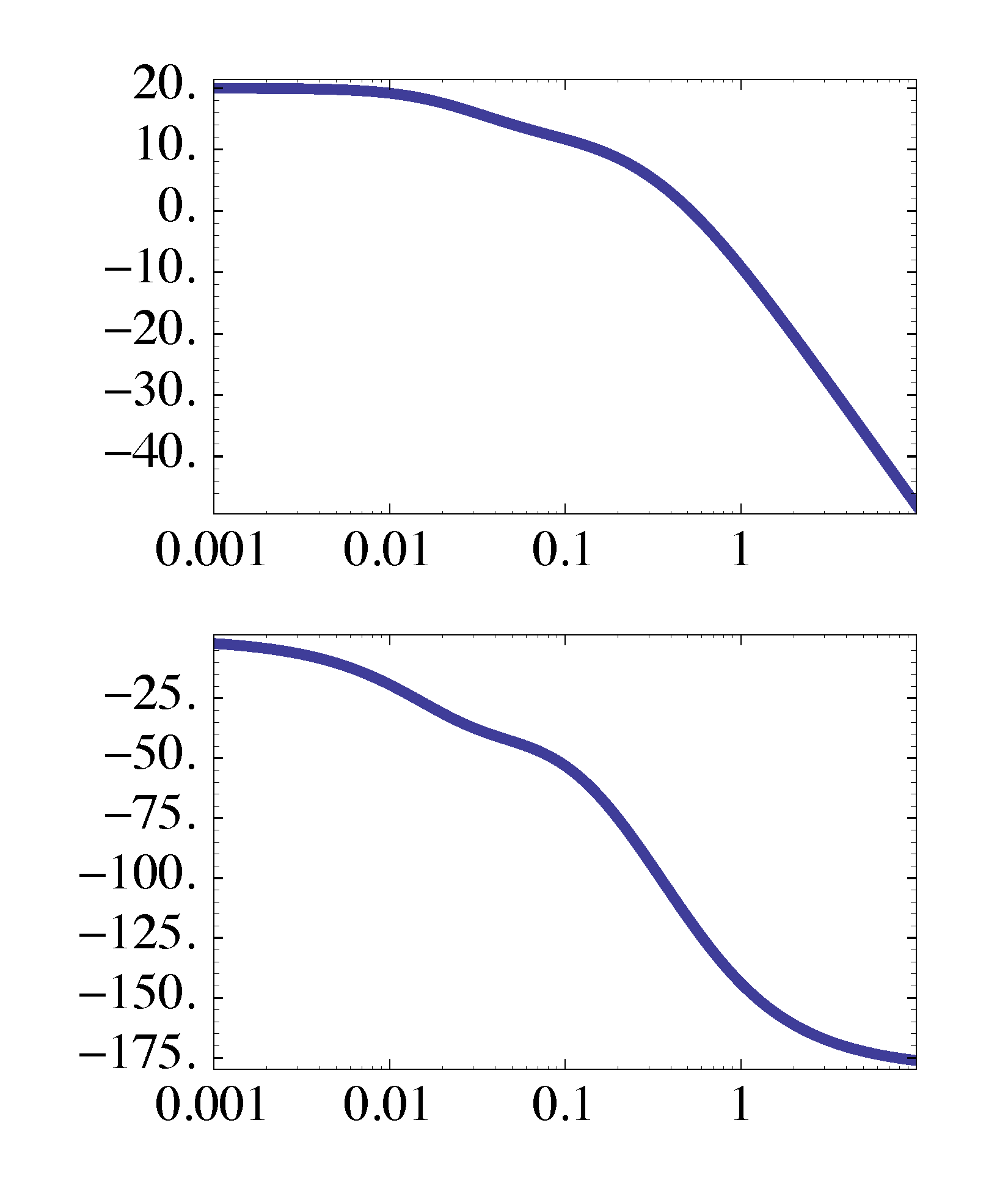
Figure 3: Bode plot for \(KD(s)G(s)\)
Lead and Lag Compensation
We can also combine the advantages of PD/lead and PI/lag control.
Consider the previous example with new objectives.
\[ G(s) = \dfrac{10}{\left(\dfrac{s}{0.2}+1\right)\left(\dfrac{s}{0.5}+1\right)}. \]
Now the new objectives are
- phase margin \({\rm PM} \ge 60^\circ\);
- bandwidth \(\omega_{\rm BW} \ge 2\);
- steady state error \(e(\infty) \le 1\%\) for tracking constant reference input.
Recall what we got before with lag alone.
- Improved phase margin by adjusting \(K\) to decrease \(\omega_c\).
- Crossover frequency decreased to \(\omega_c \approx 0.5\), whereas now we want a larger \(\omega_c\) because of \(\omega_c \leq \omega_{\rm BW} \leq 2\omega_c\); \(\omega_c = 0.5\) is too small.
We need to reshape the phase curve using lead control.
Step 1: Choose \(K\) to Adjust Crossover Frequency \(\omega_c\)
Using Figure 2, we can choose a \(K\) such that the crossover frequency \(\omega_c \approx 2\).
We can check (done by Matlab),
\[ M = |G(j\omega)| \approx 0.24 \text{ at } \omega = 2 \]
when \(K = 1\). Therefore we set \(K = \dfrac{1}{0.24} \approx 4.1667\). Roughly we can choose \(K=4\) which gives an \(\omega_c\) slightly less than \(2\).
Step 2: Choose \(z_{\rm lead}\) and \(p_{\rm lead}\) to Determine Phase Lead
With \(K=4\) already selected, we generate a new Bode plot for \(KG(s) = 4G(s)\) as shown in Figure 4.
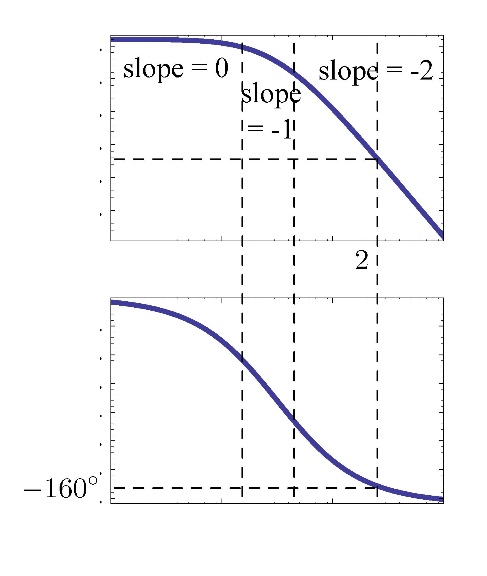
Figure 4: Bode plot for \(KG(s) = 4G(s)\)
We can check (done by Matlab),
\[ \angle 4G(j\omega) \approx -160^\circ \text{ at } \omega = 2. \]
So the phase margin is \({\rm PM} = 20^\circ\). In fact, choosing \(K=4\) increased \(\omega_c\) however it decreased the phase margin according to the phase plot.
By our design specification, we need at least \(60 - 20 = 40^\circ\) from lead component \(D(s) = \frac{s+z}{s+p}\).
The choice of lead pole and zero must satisfy
\[ \sqrt{z_{\rm lead} \cdot p_{\rm lead}} \approx 2, \text{ i.e., } z_{\rm lead} \cdot p_{\rm lead} = 4. \]
If we choose \(z_{\rm lead} = 1\) then \(p_{\rm lead} = 4\). The resulting lead component is \(\displaystyle D(s) = \frac{s+1}{\frac{s}4+1}\). (Why not \(D(s) = \frac{s+1}{s+4}\)? Hint: \(K=4\) is already set; the DC gain of \(D(s)\) needs to be \(1\).)
We can double check the phase bump contributed by \(D(s) = \frac{s+1}{\frac{s}4+1}\).
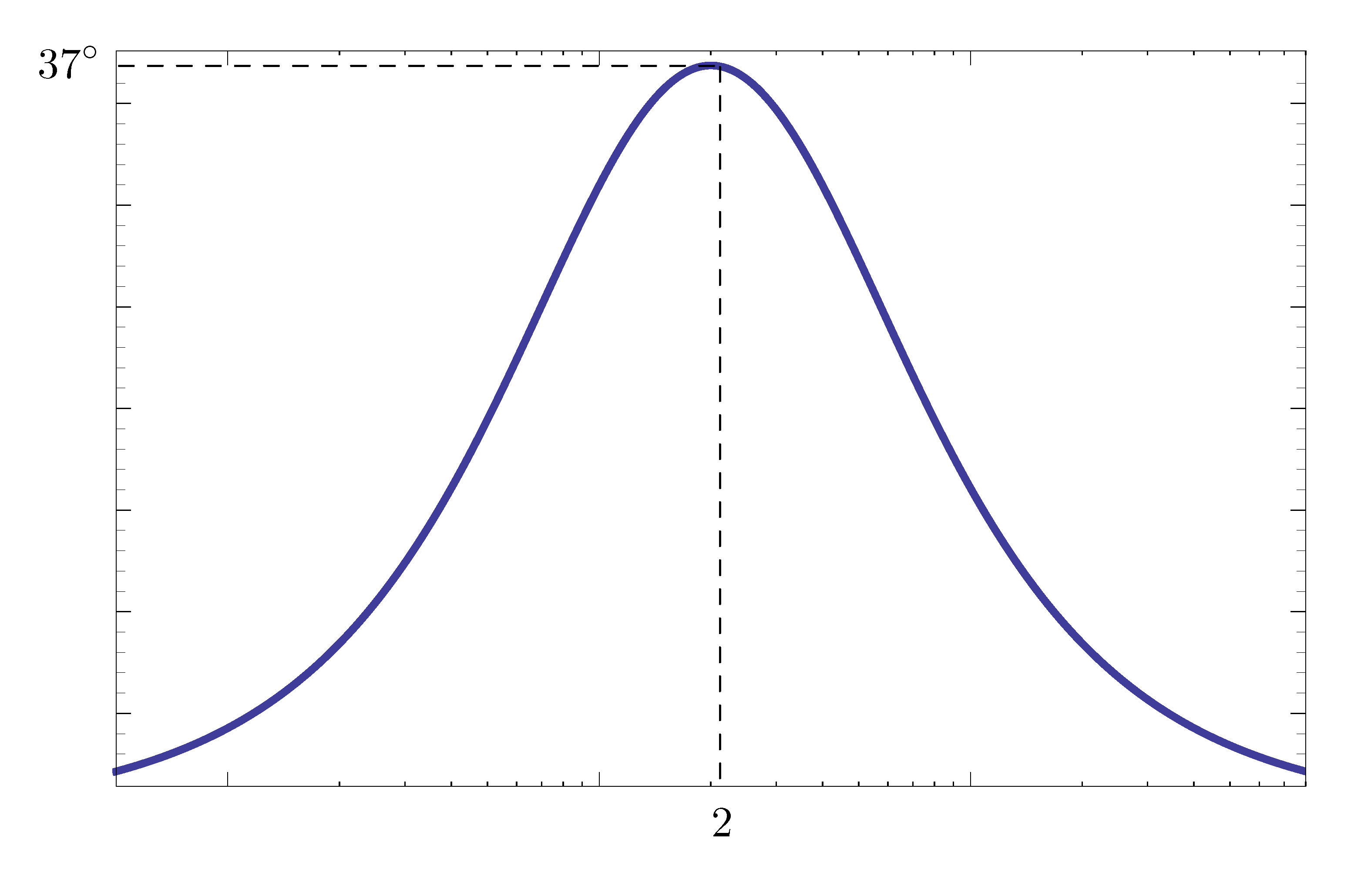
Figure 5: Phase plot for \(D(s) = \frac{s+1}{\frac{s}4+1}\)
By Figure 5, there is not enough phase lead from \(D(s)\) by previous design attempt.
We can space \(z_{\rm lead}\) and \(p_{\rm lead}\) farther apart. By widening the gap between \(z\) and \(p\), we can make the maximum angle of \(D(s)\) increase. For example,
\begin{align*} \begin{cases} z_{\rm lead} = 0.8 \\ p_{\rm lead} = 5 \end{cases} \implies \text{phase lead } = 46^\circ. \end{align*}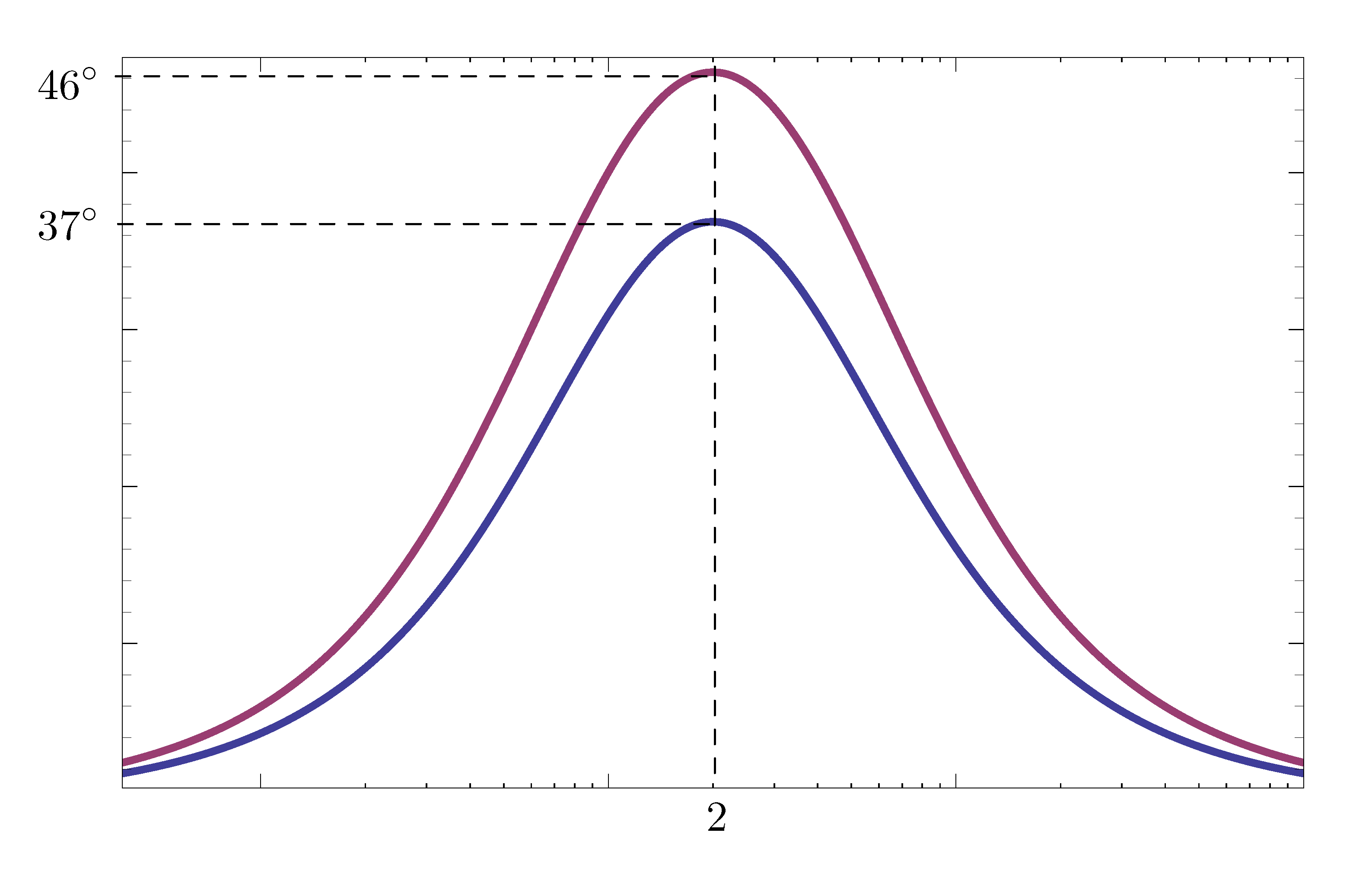
Figure 6: Overlaid phase plot for both \(D(s) = \frac{s+1}{\frac{s}4+1}\) and \(D(s) = \frac{\frac{s}{0.8}+1}{\frac{s}5+1}\)
Step 3: Overall Design and Confirmation of Specifications
Now we need to evaluate the steady state tracking error with the chosen \(K\), \(z_{\rm lag}\) and \(p_{\rm lag}\).
The equivalent open loop transfer function now is
\begin{align*} K\underbrace{D(s)}_{\text{lead} \atop \text{only}}G(s) &= 4 \frac{\dfrac{s}{0.8}+1}{\dfrac{s}{5}+1} \cdot \frac{10}{\left(\dfrac{s}{0.2}+1\right)\left(\dfrac{s}{0.5}+1\right)}. \\ KD(0)G(0) &= 40 \implies e(\infty) = \frac{1}{1+KD(0)G(0)} = \frac{1}{1+40}. \end{align*}Hence the tracking error is not small enough. Specification requires error less than \(1\% =\dfrac{1}{100} = \dfrac{1}{1+99}\). Therefore
\begin{align*} D(0) &\ge \frac{99}{KG(0)}\\ & = \frac{99}{40}. \end{align*}Keeping the ratio \(\frac{z_{\rm lag}}{p_{\rm lag}} \approx 2.5\) will suffice to achieve our goal. Note we need to choose lag pole/zero that are sufficiently small in order not to distort the phase by lead component too much. Another way to see it is that \(\angle\frac{s + z_{\rm lag}}{s + p_{\rm lag}} \approx 0\) when both \(z_{\rm lag}\) and \(p_{\rm lag}\) are small.
Now the overall controller becomes
\begin{align*} \tag{2} \label{d17_eq2} KD(s) &= \underbrace{4}_{\triangleq D_p} \cdot \underbrace{\frac{\dfrac{s}{0.8}+1}{\dfrac{s}{5}+1}}_{ \triangleq D_d} \cdot \underbrace{\frac{s+0.05}{s+0.02}}_{\triangleq D_i} \\ &= D_p D_d D_i, \\ \end{align*}where \(D_d\) is the lead component and \(D_i\) is the lag component.
Notice \(KD(s)\) in Equation \eqref{d17_eq2} is comparable to a PID controller in the sense that the lead component is an approximate PD control (associated with control of damping) and the lag component is an approximate PI control (associated with control of steady state error).
In summary, when we tried to design a lead-lag compensator, we started with \(D_p = K\) which shaped the crossover frequency. Then by the requirement of phase margin, we further stacked a lead component \(D_d = \frac{\frac{s}{z_{\rm lead}}+1}{\frac{s}{p_{\rm lead}}+1}\) to \(D_p\). At last by the requirement of steady state error, we appended a lag component \(D_i = \frac{s + z_{\rm lag}}{s + p_{\rm lag}}\).
Frequency Domain Design Method: Advantages and Disadvantages
Based on the examples above, we see the design based on Bode plots is good for
- easily visualizing the concepts;
- evaluating the design and seeing which way to change it;
- using experimental data. (Frequency response of an undocumented system can be measured experimentally, called system identification. cf. Lab 4 and Lab 6.)
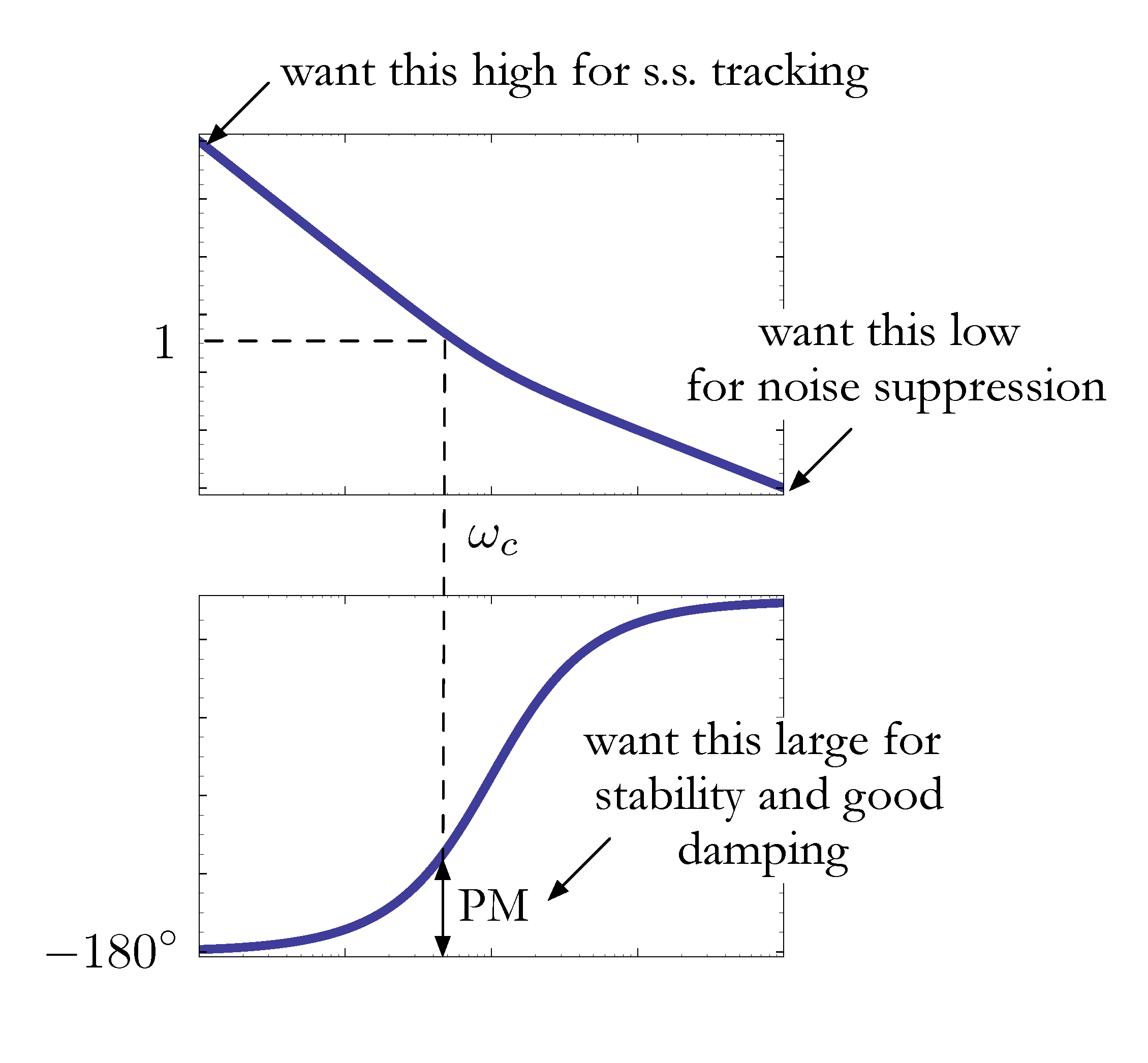
Figure 7: Bode plot as a design guideline for loop shaping
While the design based off of Bode plots is very geometric, it is not so good for
- exact closed loop pole placement (root locus might be more suitable for that);
- deciding if a given \(K\) is stabilizing or not.
- We can only measure how far we are from instability using gain margin or phase margin, if we know that the systems are stable.
- However, we do not have a way of detecting whether a given \(K\) is stabilizing from frequency response data.
What we want is a frequency domain substitute for the Routh–Hurwitz criterion: the Nyquist stability criterion, which will be discussed in the next lecture.