
The main purpose of this assignment is to (a) give you experience building and using a simulator software and (b) to get you thinking about architecture quantitatively.
The following figure describes the data cache system for a particular microprocessor. We know that the processor consists of a simple in-order pipeline that blocks on L1 cache misses. We know very little about the caches of this system except that the L1 cache, if it is associative, uses the Least Recently Used (LRU) replacement policy. We also know that the latency between the L1 and L2 cache is p cycles.
In order to discover the size and organization of the L1 data cache, we have decided to run a small code kernel on it, which is described in pseudo code below. The code sequentially accesses D elements of an array called A repeatedly 100 times.
        do 100 times {
          for i = 0 to D-1 {
            access A[i];
          }
        }
By running this small loop for various values of D, we are able to obtain a graph of the average latency for an access to the array A. The graph is shown below.
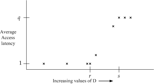
Using the values q, r, and s derived from this graph, along with p (L2 cache latency), determine the following properties of the L1 cache: (a) hit latency, (b) size, (c) line size, (d) associativity.
What (if anything) do you learn by running the loop from Problem 1 on your laptop (or any other computer to which you have access)? Explain.
Average memory latency has been increasing for the last 10 years, relative to the rest of the processor, even though caches are getting much larger. This is because, while logic transistors have sped up by a factor of about 8, DRAM speeds have increased by only about a factor of 2. Thus a DRAM access today takes about 4 times more gate delays today than it did in 1994.
Let's test the above assertion. After you unpack, build and run an architecture simulator, use the command line parameters to model memory systems similar to those seen in 1994 and in 2007. I recommend using Simplescalar or M5
You should model two memory systems. For 1994 era memory assume 16K L1 I and D caches, no L2 cache, and DRAM access cost of 30 cycles. For a 2008 era memory system model an L2 cache and a DRAM access cost of 120 cycles (similar to assuming that we took a c. 1994 pentium netlist added an L2 cache to take advantage of our larger transistor budget and fabbed it on a state-of-the-art 2004 fab). You'll have to make some assumptions about L2 hit latency. One reasonable assumption is that SRAM latency is sqrt(size/16384). Thus a 64K L2 would have a 2 cycle latency, 256K => 4 cycles, 1M => 8 cycles, 4M => 16 cycles, 16M => 32 cycles.
What happens as you change your data cache orgranization? Does the number of cycles to execute the program increase or decrease, and by how much?
Recall that the formula for average memory latency is:
h lh + (1 - h) lm
where h is hit-rate, lh is hit latency, and lm is miss latency. What hit rate would you need to achieve to completely make up for the relative increase in DRAM latency?
Each person should turn in a short (1-2 pages for assignment 1) report on what you implemented and what you learned. You should address questions like the following: What assumptions did you make? What did you try that didn't work? Which of the changes you made were most and least effective? For those features that weren't very effective, why do you think they didn't work very well?
Next Wednesday: 3rd September