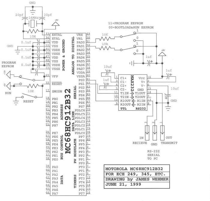
| HC912 Chip Pin #'s - In order as they appear on the ECE module |
Description |
| Pin 35 |
(LSTRB)'/PE3 - Low-Byte Strobe/Port E |
| Pin 37 |
(IRQ)'/PE1 - Maskable Interrupt Request pin/High voltage supply to EEPROM used for test purposes only in Special modes/Port E |
| Pin 39 |
ADDR8/DATA8/PA0 - External Address/Data Bus/Port A |
| Pin 41 |
ADDR10/DATA10/PA2 - External Address/Data Bus/Port A |
| Pin 43 |
ADDR12/DATA12/PA4 - External Address/Data Bus
|
| Pin 45 |
ADDR14/DATA14/PA6 - External Address/Data Bus/Port A |
| Pin 47 |
VDD - Internal power and ground |
| Pin 49 |
VRH - Reference voltages for the analog-to-digial converter |
| Pin 51 |
PAD0/AN0 - Port AD/Analog inputs |
| Pin 53 |
PAD2/AN2 - Port AD/Analog inputs |
| Pin 55 |
PAD4/AN4 - Port AD/Analog inputs |
| Pin 57 |
PAD6/AN6 - Port AD/Analog inputs |
| Pin 59 |
VDDA - Operating voltage and ground for the analog-to-digital converter, allows the suppply voltage to the A/D to be bypassed independently |
| Pin 61 |
PS0 - Port Signals |
| Pin 63 |
PS2 - Port Signals |
| Pin 65 |
PS4 - Port Signals |
| Pin 67 |
PS6 - Port Signals |
| Pin 69 |
VFP - Programming voltage for the Flash EEPROM and required supply for normal operation |
| Pin 71 |
PDLC5 or PCAN5 - Port CAN |
| Pin 73 |
PDLC3 or PCAN3 - Port CAN |
| Pin 75 |
PDLC1 or TxCAN - transmit Port CAN |
| Pin 77 |
VSSX - External power and ground, supply to pin drivers |
| Pin 79 |
PP7 - Port P |
| Pin 01 |
PP5 - Port P |
| Pin 03 |
PW3/PP3 - Pulse Width Modulator channel outputs/Port P |
| Pin 05 |
PW1/PP1 - Pulse Width Modulator channel outputs/Port P |
| Pin 07 |
IOC0/PT0 - input capture and output compare/Port T |
| Pin 09 |
IOC2/PT2 - input capture and output compare/Port T |
| Pin 11 |
VSS - Internal power and ground |
| Pin 13 |
IOC4/PT4 - input capture and output compare/Port T |
| Pin 15 |
IOC6/PT6 - input capture and output compare/Port T |
| Pin 17 |
SMODN/BKGD - Mode Select/single-Wire Background Mode Pin |
| Pin 19 |
ADDR1/DATA1/PB1 - External Address/Data Bus
|
| Pin 21 |
ADDR3/DATA3/PB3 - External Address/Data Bus/Port B |
| Pin 23 |
ADDR5/DATA5/PB5 - External Address/Data Bus/Port B |
| Pin 25 |
ADDR7/DATA7/PB7 - External Address/Data Bus/Port B |
| Pin 27 |
MODB/IPIPE1/PE6 - Mode Select/Instruction Queue Tracking Signals/Port E |
| Pin 29 |
ECLK/PE4 - E-Clock Output/Port E |
| Pin 31 |
VDDX - External power and ground, supply to pin drivers |
| Pin 36 |
R/(W)'/PE2 - Read/Write/Port E |
| Pin 38 |
(XIRQ)'/PE0 - Nonmaskable Interrupt/Port E |
| Pin 40 |
ADDR9/DATA9/PA1 - External Address/Data Bus/Port A |
| Pin 42 |
ADDR11/DATA11/PA3 - External Address/Data Bus/Port A |
| Pin 44 |
ADDR13/DATA13/PA5 - External Address/Data Bus/Port A |
| Pin 46 |
ADDR15/DATA15/PA7 - External Address/Data Bus/Port A |
| Pin 48 |
VSS - Internal power and ground |
Pin 33 |
EXTAL - External Clock Input |
| Pin 34 |
XTAL - Crystal Driver |
| Pin 50 |
VRL - Reference voltages for the analog-to-digial converter |
| Pin 52 |
PAD1/AN1 - Port AD/Analog inputs |
| Pin 54 |
PAD3/AN3 - Port AD/Analog inputs |
| Pin 56 |
PAD5/AN5 - Port AD/Analog inputs |
| Pin 58 |
PAD7/AN7 - Port AD/Analog inputs |
| Pin 60 |
VSSA - Operating voltage and ground for the analog-to-digital converter, allows the suppply voltage to the A/D to be bypassed independently |
| Pin 62 |
PS1 - Port Signals |
| Pin 64 |
PS3 - Port Signals |
| Pin 66 |
PS5 - Port Signals |
| Pin 68 |
PS7 - Port Signals |
| Pin 70 |
PDLC6 or PCAN6 - Port CAN |
| Pin 72 |
PDLC4 or PCAN4 - Port CAN |
| Pin 74 |
PDLC2 or PCAN2 - Port CAN |
| Pin 76 |
PDLC0 or RxCAN - receive Port CAN |
| Pin 78 |
VDDX - External power and ground, supply to pin drivers |
| Pin 80 |
PP6 - Port P |
| Pin 02 |
PP4 - Port P |
| Pin 04 |
PW2/PP2 - Pulse Width Modulator channel outputs/Port P |
| Pin 06 |
PW0/PP0 - Pulse Width Modulator channel outputs/Port P |
| Pin 08 |
IOC1/PT1 - input capture and output compare/Port T |
| Pin 10 |
VDD - Internal power and ground |
| Pin 12 |
IOC3/PT3 - input capture and output compare/Port T |
| Pin 14 |
IOC5/PT5 - input capture and output compare/Port T |
| Pin 16 |
PAI/IOC7/PT7 - Pulse accumulator input/input capture and output compare/Port T |
| Pin 18 |
ADDR0/DATA0/PB0 - External Address/Data Bus/Port B |
| Pin 20 |
ADDR2/DATA2/PB2 - External Address/Data Bus/Port B |
| Pin 22 |
ADDR4/DATA4/PB4 - External Address/Data Bus
|
| Pin 24 |
ADDR6/DATA6/PB6 - External Address/Data Bus/Port B |
| Pin 26 |
(DBE)'/PE7 - Data Bus Enable/Port E |
| Pin 28 |
MODA/IPIPE0/PE5 - Mode Select/Instruction Queue Tracking Signals/Port E |
| Pin 30 |
VSSX - External power and ground, supply to pin drivers |
| Pin 32 |
(RESET)' - reset |