| Name | NetID | Section |
|---|---|---|
| Jerry Chang | chiehc3 | ECE 120 |
| Shinan Calzoni | calzoni2 | ECE 120 |
Statement of Purpose
The purpose of this project is to learn about sequential logic design by combining storage and display elements with combinational logic in order to make a 24-hour digital clock.
The catch is that we will mostly be using logic gate ICs with a few exceptions (multiplexers, decoders, flip-flops).
Background Research
Our original project idea involved the creation of an ALU, however, after realizing our project would essentially be one of the ECE 385 labs, we decided to extend the project with the creation of a digital clock, which would also require some form of an ALU.
In our digital clock, we will implement a sequential logic design which is a synthesis of combinational logic structures and storage elements, or in other words, components that process data and components that store data. Combinational logic structures are generally composed of various digital logic which may include multiplexers (muxes), full adders, decoders, etc. The important idea is that all combinational logic is at its base made solely using logic gates. With regards to the storage elements involved in our project, we will be using a variation of a flip-flop which allows a value to be temporarily stored while an incoming value is processed.
Finally, the time of our digital clock will be made visible using multiple seven-segment displays which are very common in many electronic devices. This method of representation consists of seven LEDs that each light up according to the number/letter that is required to be displayed.
Block Diagram / Flow Chart
Original Flow Chart :
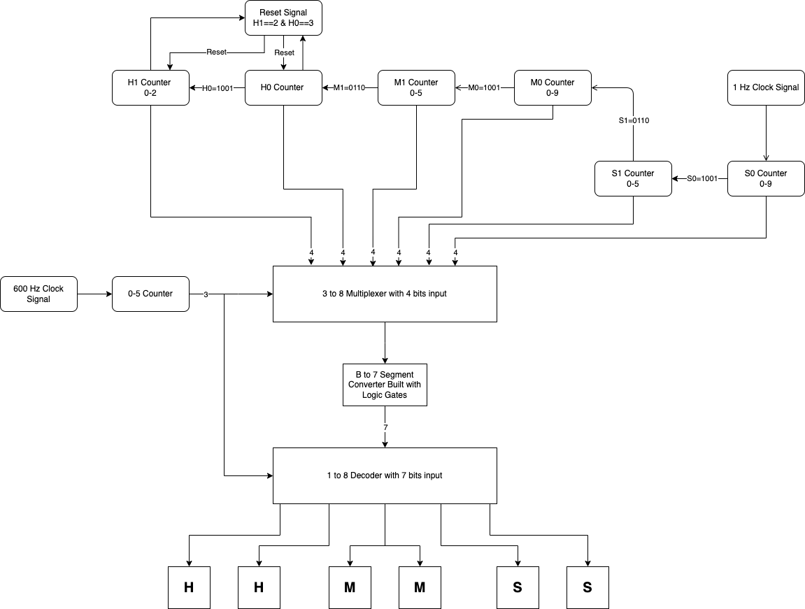
Revised Flow Chart :
System Overview
Paper: https://docs.google.com/document/d/1ugc-kp7VbF0n179fc4Owe8xM8YEdW0l5BseCyaLPQAs/edit?usp=sharing
Video: https://drive.google.com/file/d/1SBBHzjQVVKI34sex5FU6DpNg49SoZOxX/view?usp=sharing
Circuit Design Snapshot: https://simulator.io/board/xxZu4xxX5X/2
Digital Clock:
Our project was inspired by an article posted on instructables.com (see references). In the article, the development of a 12-hour clock and alarm is detailed, however, in our project, we will not be including an alarm, our time will be represented with military time, and our design will have an important difference.
Since our digital clock will be designed mainly using logic gates, we will build a B to 7S converter ourselves using NAND gates and inverters. There are six digits in the clock, however, rather than building six B to 7S circuits, we decided that it would be more efficient to use a single circuit for the six digits by implementing a 0-5 counter (for each clock digit) attached to a 600 Hz clock signal. The reason for the high frequency is so the LEDs will flash at a high enough rate for it to be unnoticeable to the human eye.
The signals to each digit will be controlled with four 8:1 muxes with each mux representing four bits of any given digit as well as 7 3:8 decoders which will control the digit that is currently being illuminated. The control signals of the muxes and decoders will be connected to the 0-5 counter operated by a 600 Hz signal that was mentioned above.
For the SS part (Seconds), we use two 0-9 counters to represent the second of time in our clock. The 1 Hz clock signal will signal the S0 counter to add 1 every second. Whenever the S0 counter reaches 9, it will signal the S1 counter to increment by one. Whenever the S1 counter reaches 5 and is about to reach 6, it will signal the M0 counter to increment by 1. The same thing occurs between the M0 and M1 digits. When the M1 digit and M0 digit display 5 and 9, respectively, the H0 digit will increment by 1. Finally, when the H0 digit reaches 9, the H1 digit will increment by one. Using this logic, we can build a clock with HH:MM:SS displaying military time.
Parts
-Breadboards
-Power supply
-Seven-segment display (6)
140101250 : 7-SEG READOUT COMMON ANODE
-Logic Gates, Flip-Flops, Decoders, etc:
SN74175N : D-F/F Quad (6)
74LS151 : MUX 1 to 8 (4)
74LS157 : MUX Quad 2 to 1 (4)
Possible Challenges
Designing the circuit
Execution of the design
Debugging the circuit
References
[1]M. », "Learning Sequential Logic Design for a Digital Clock", Instructables, 2021. [Online]. Available: https://www.instructables.com/Digital-Clock-Sequential-Logic-Design/. [Accessed: 26- Sep- 2021].
Ben Eater : ALU Design
Github Repo : ECE-385/ECE 385 Lab Report 3.pdf at master · OfficialPouya/ECE-385
555 timer calculator https://www.daycounter.com/Calculators/NE555-Calculator.phtml


